

Information Technology (IT) Pioneers
Retirees and former employees of Unisys, Lockheed Martin, and their heritage companies
32-bit Computers, Chapter 55
1. Introduction
The LEGACY computers are listed by Instruction Set Architecture bit length because the ISA established a thread of commonality and similarity through a line of systems. This led to commonality of support software, experienced programmers, and commonality of maintenance engineer knowledge, and customer confidence in operational reliability. [lab]
2. Computer Family
AN/UYK-7, AN/AYK-10, CP-140, and AN/UYK-43. These computers had a bootstrap (core rope) designed-in diagnostic capability, see the AN/UYK-7 NDRO function card. The AN/UYK-43 had a designed in maintenance processor.
Note that the Nike Tactical Intercept Computer (TIC) and the CLC successor were 32 bits also, but a different ISA than the above Navy computers. Those are discussed on the Computers, Special Purpose - Chapter 58.
3. Computer Descriptions
3.1 AN/UYK-7
The project started April 1968, first delivery 4/21/1969.
The AN/UYK-7 standard shipboard computer was designed in accordance
with stringent military specifications as to performance and ruggedness.
The U.S. Navy was the developing government agency. The architecture
came out of a study by UNIVAC;
Another
Computer Was Born by Curt Christensen.
The AN/UYK-7 became the heart of the NTDS second generation
system, replacing the aging AN/UYK20Bs while implementing an architecture
capable of supporting multiple I/O controllers and having multiple processors
sharing memory and software tasks. Innovations in this design are numerous,
i.e. an eight port memory that allowed three processors and two I/O
controllers to be accessing memory concurrently as long as the address
requests were to different memory banks. The first enhancement to the
AN/UYK-7 was the implementation of a film memory chassis which created
a 32k word memory in the same volume as the initial 16-k core memory
chassis. The film memory technology was adapted from the AN/AYK-10's
memory design. Each memory chassis had eight memory buses. In a multi-processor
configuration; three instruction fetches, three operand fetches, and two I/O word transfers
could take place simultaneous if all were referencing different memory
banks. 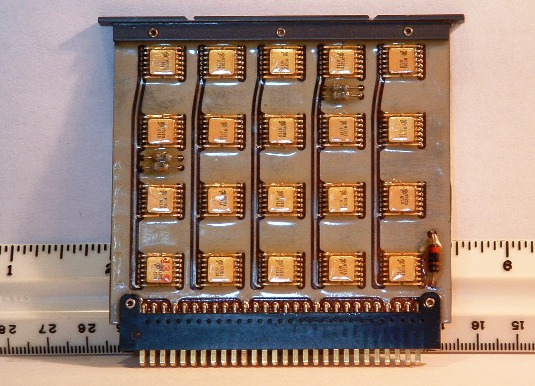 The UYK-7 design used the heat sink, T-bar card design and heat
exchanger design from the CP-901. The integrated circuit flat packages
were mounted onto a conductor which carried chip heat to the T-bar at
the top. When inserted into chassis, a heat exchanger plate was clamped
to the chassis. Air forced through the heat exchanger cooled the unit.
The typical operating temperature of components on this card type was
30 degrees above ambient.
The UYK-7 design used the heat sink, T-bar card design and heat
exchanger design from the CP-901. The integrated circuit flat packages
were mounted onto a conductor which carried chip heat to the T-bar at
the top. When inserted into chassis, a heat exchanger plate was clamped
to the chassis. Air forced through the heat exchanger cooled the unit.
The typical operating temperature of components on this card type was
30 degrees above ambient.
The lead logic designer from the CP-901, Ken Oehlers, also became
the lead processor designer for the UYK-7. John Bonnes also joined
the design team for this computer as the CP-901 checkout lead was taken
over by Lowell Benson. A common executive program facilitated operational
programming. [lab]
Comments From: Rick Orozco via web site on 23 January, 2009.
Hi, Thank you for the interesting web site. I was a UYK-7 computer tech
for the US Navy from 1989-2000. I enjoyed learning the system inside
and out and was a fairly good programmer in machine language. On the
USS John Rodgers DD-983, we had a "spare" stand alone bay, which I actually
wrote about a 10,000 line word processing program for use at our teletype.
Of course this was right before the introduction of the PC, so it came
in handy.
I also worked on the CP-642 when stationed onboard the USS Midway CV-41. In fact, in the picture of the SINS computer on your web site, you can still see my notes for reloading the computer, the little white index card posted on the control panel. {Editor's note: see section 3.6 of Computers, 30-bit.} Thanks to the many great engineers and programmers that created these systems and helped to make our military the best in the world. Rick Orozco, Chief Data Systems Technician, US Navy Retired
3.2 Unisys Type 1832, AN/AYK-10
Also called the S-3A computer, the nomenclature of the airplane it
was designed to fit into.
This project started in 1969 with first delivery September 14,
1970. The AN/AYK-10 is a dual processor, dual I/O controller airborne
version of the UYK-7 ISA with
special I/O used for ASW missions aboard the Lockheed S-3A carrier based
aircraft. Innovations of this design: 1) dual mated film memory
chassis running at 1.5 microseconds - each with 6 access ports. 2) a
dual processor design interconnected so that if one CPU or one memory
chassis or one I/O chassis failed, the system would continue to operate
in a reduced capacity mode. Thus a reduced flight mission could continue
- maybe just track 3 sono-buoys instead of 6 to 8, etc. 3) a unique
frame design that fit at the rear of the S-3A crew compartment - the
wheels folded up almost against the sides of the Power Supply and third
memory drawer.
Don Mager was the project engineer, Gary Bosworth
and Gerry Shaw were two of the logic design engineers on this project. The
operational software was developed by Sperry at the Valencia operations
building. The first computer was delivered on 9/14/1970. There were
a total of 205 of these computers built, including those for the
Canadian CP-140.
[lab]
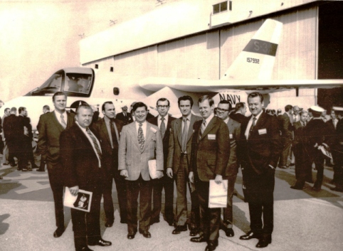
Photo submitted by Jim Rapinac. Sperry Univac DSD attendees,
L-R present at the first aircraft roll-out were:
- Jim Rapinac, General Manager, Special Programs, Salt Lake City
- Bill McGowan, Marketing Rep, LA office
- Ernie Hams, VP Program Management
- Dick Gehring, VP and General Manager in St. Paul
- Ken Oehlers, S-3A Engineering Director
- Dan Brophy, S-3A Program Manager
- Dewaine Osman, VP Marketing
- John Spearing, DSD Valencia Site Manager
- Norbert Kielbach, Marketing Rep, LA office

Feedback to webmaster:
I just finished a biography on Lockheed and then read a pdf report titled
"50 Years of Ocean Surveillance" edited by Lowell A. Benson
(no idea how I got that on my phone). I can relate a lot to what I read.
I was never aware of your group and what you are doing. {Editor's note:
http://vipclubmn.org/Articles/OceanSurveillance.pdf}
I worked for Lockheed in Burbank, CA and was developing automatic testing programs for the S-3A computer and
spectrum analyzer starting in 1972 at the Rye Canyon Research Facility in Valencia, CA.
By the mid 1970's I was transferred to Lockheed's Advanced Design Group where
I had opportunities to develop and test algorithms for detecting and
tracking of submarines. I remember having to punch my own cards and feed them into a
UNIVAC system to compile the assembly code. The room had to be freezing cold in the
1960's otherwise the UNIVAC computer would overheat and crash. The compiled code was written out
onto paper tape which was used to feed into an S-3A mock-up system in the lab on which
I could test out my ideas. I usually had to go to the lab during the night so
I had the system all to myself, getting home around 5 am after having been working all day.
Jerry Ehlers, PhD [feedback item added 12/21/2020]
3.3 The CP-140
This is the Canadian Patrol aircraft developed for their Aurora program. It is essentially the Canadian version of the P-3C for their ASW missions. Instead of the CP-901 computer, it used the Sperry 1832 three memory chassis instead of the two used aboard the US Navy's S-3A. The Canadian government nomenclature assigned to this machine was AN/AYK-502, not to be confused with the later AN/UYK-502 shipboard mini-computer.
3.4 S-3B Systems Computer
 The
Type 1832 (AN/AYK-10) enhanced version implemented a doubled capacity
semiconductor memory chassis [designed for the Canadian AN/AYK-502]
to upgrade the original film memory drawers. I, Lowell, was the engineering manager
for the memory proposal and development. I do not recall who the design engineering team was -
we transferred the build to Winnipeg.
The
Type 1832 (AN/AYK-10) enhanced version implemented a doubled capacity
semiconductor memory chassis [designed for the Canadian AN/AYK-502]
to upgrade the original film memory drawers. I, Lowell, was the engineering manager
for the memory proposal and development. I do not recall who the design engineering team was -
we transferred the build to Winnipeg.
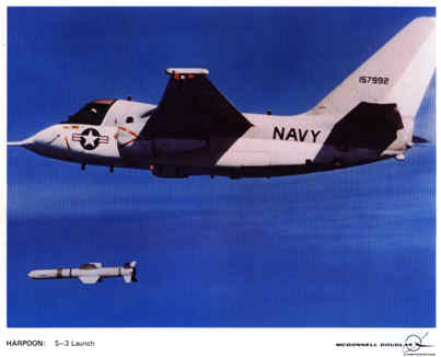
 The aircraft nomenclature was upgraded to S-3B because Sperry Univac also
did a design update to the Input/Output Controllers to effect a Harpoon
missile launch capability. The four 6" x 6" PC cards weighed just three
lb. instead of the MacDonald Douglas 40 lb. launch computer used aboard
the P-3C. The power consumption of this feature was an additional five
watts compared to the 200 watts of the stand-alone launch computer on
the P-3C. Gerry Shaw, Gary Bosworth, and I did the technical work on
the proposal. When we received the contract; Ken Graber and Mark Nelson
did most of the logic and electrical design of the launch interface. One of the new cards provided the missile with targeting data and
the second card was the launch control, i.e. firing/release.
The aircraft nomenclature was upgraded to S-3B because Sperry Univac also
did a design update to the Input/Output Controllers to effect a Harpoon
missile launch capability. The four 6" x 6" PC cards weighed just three
lb. instead of the MacDonald Douglas 40 lb. launch computer used aboard
the P-3C. The power consumption of this feature was an additional five
watts compared to the 200 watts of the stand-alone launch computer on
the P-3C. Gerry Shaw, Gary Bosworth, and I did the technical work on
the proposal. When we received the contract; Ken Graber and Mark Nelson
did most of the logic and electrical design of the launch interface. One of the new cards provided the missile with targeting data and
the second card was the launch control, i.e. firing/release.
Especially tricky was the Failure Modes and Effects Analysis
which Mark did. He had to determine how the failure of any component
would manifest itself, i.e. not allow the system to launch or accidently
launch the missile. No single component failure could launch! Good job
with the design Mark and Ken. [lab]
![]()
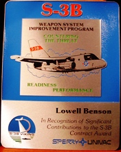
In April 2025, I toured the USS Yorktown aircraft carrier -museum- in Charleston SC. On deck was an S-3B with an information plaque:
.JPG)
.JPG)
The Harpoon missiles were carried on the vertical 'stallions' just inside
the wing fold. LABenson
3.5 AN/UYK-43, updated November 2025
Updates to this section were provided by Bob Jablonski, Doug Wiedenman, John Westergren,
and Don Leichtweis, Capt. USN Ret. with editing by Mary Beth Ruhland and formatting by Lowell Benson.
The new subsections are: Contract Competition,
Development, Deliveries, and an
Enduring Legacy.
In situations when an incoming missile or aircraft are threatening a vessel, microseconds become critical.
Making timely, accurate, quick decisions saves lives. The Navy's requirement specifications and subsequent design of each of the AN/UYK-43
development areas described below was performed cohesively in concert to achieve that real-time response.
3.5.1 Contract Competition
The AN/UYK-43 was conceived in Washington, D.C. by the Navy’s engineers in the late 70s. Then Cdr. Don Leichtweis was tasked by Capt. Carl Drenkard to perform a study and to draft a requirements document for a next generation computer. He, Don, gathered inputs from all Navy Program offices (NavSea, NavElex, and NavOrd) as well as from numerous Navy laboratories around the country. Then in the early 80s a competitive solicitation and eventual “fly-off” was conducted between the two premier computer developers at the time, International Business Machines (IBM) and Sperry UNIVAC. Development contracts were awarded in September 1980, then the production contract was won by Sperry UNIVAC on May 27, 1983. Sperry Defense Systems Division subsequently became Unisys/Loral/Lockheed Martin. Our Stories posted July 2007, https://vipclubmn.org/Articles/CPFwin.pdf, page 4 relates the AN/UYK-43 contract win, written by Michael A. Bukovich
3.5.2 Development
The AN/UYK-43 is the third generation Naval Tactical Data System (NTDS) large-scale mainframe computer that was specified as the emerging
AN/UYK-7 replacement, .
UNIVAC had also provided the computers for the Navy’s first two
generations, starting with responding to the Navy’s requirements in
the 1950s for a general-purpose, real-time, shipboard, multipurpose,
programmable computer. [first generation USQ-17 and
USQ-20 computers had transistor electronics and second generation UYK-7 had integrated circuit electronics,
https://vipclubmn.org/cp32bit.html#UYK7].
The UYK-43’s innovations included a designed-in maintenance processor*, cache memory for performance enhancements, plug-in North Atlantic
Treaty Organization (NATO) serial interface, Instruction Set
Architecture (ISA) improvements, fault/failure tolerance, and
numerous manufacturing innovations. Much of the logic design was
implemented using gate array technologies. Many of these innovations
pushed the state-of-the-art beyond what was previously available.
Even though its basic architecture and design was complete in the mid-1980s, it was still performing in
multiple mission critical combat systems throughout the surface and
subsurface Navy 30+ years later. [John Westergren]
*The maintenance processor was the result of an Internal Research
& Development (IRAD) project; item 3 on page 12 of
https://vipclubmn.org/PeopleDocImg/Vol1Book01.pdf.
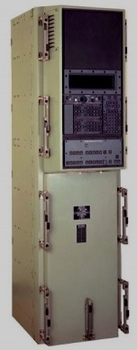 Packaging: Since the UYK-43 was destined to become the Navy’s
standard computer for multiple systems, it needed to be easily
installed on both surface ships and submarines. The submarine
requirement caused the unit’s physical size to be designed to fit
through a standard submarine hatch, and the unit was subsequently
loaded onto many vessels like torpedoes were loaded. This single
requirement demanded that a number of innovative packaging
approaches be taken, with eventual manufacturing and production
challenges, each meeting the Navy’s requirements of the day.
Packaging: Since the UYK-43 was destined to become the Navy’s
standard computer for multiple systems, it needed to be easily
installed on both surface ships and submarines. The submarine
requirement caused the unit’s physical size to be designed to fit
through a standard submarine hatch, and the unit was subsequently
loaded onto many vessels like torpedoes were loaded. This single
requirement demanded that a number of innovative packaging
approaches be taken, with eventual manufacturing and production
challenges, each meeting the Navy’s requirements of the day.
- Cooling: The dense packaging of electronics in the UYK-43 enclosure generated a huge amount of heat. The most efficient method of removing that heat from the unit was through a complex method of heat exchangers to a water-cooling system, and on to the ship’s cooling system. This significantly increased the ability to tightly package the electronics while keeping them at an efficient operating temperature that extended their life and optimized their performance.
- Instruction Set: Computers execute instructions as defined by their program and programmers. The AN/UYK-43 utilized the basic instructions previously developed for its AN/UYK-7 predecessor, taking full advantage of the huge investment already made by the Navy in mission critical application programs. More efficient instructions were also developed for the AN/UYK-43 to improve the computational capability of the processor: floating point arithmetic, trigonometric functions, etc. The combination of improved memory access, gate array, and packaging techniques took giant leaps in technology to improve processing performance speed. The support software was also upgraded to take advantage of the new capabilities and technology.
- Processing: No processor packed more power and capability into such a small package as the UYK-43. Only later, as processing technology continued to improve, were others able to attain the levels of performance provided by the UYK-43 to the Navy’s many applications.
-
Gate Arrays: The UYK-43 lead the usage of Large-Scale Integration (LSI) gate arrays where hundreds of thousands (eventually millions)
of integrated circuits can be produced on a single piece of silicon. This greatly increased the speed and efficiency of performing
the computer instructions and calculations which previously used discrete/individual logic circuit devices.
UYK-43’s usage of LSI significantly increased performance and the ability of mission-critical defensive or offensive systems to respond to demands much more effectively.
This was proven again and again; in 2008 with the destruction of a failing satellite by the Aegis cruiser, USS Lake Erie. The UYK-43 computer is the central processor for the Aegis combat system which allowed a SM-2 missile to have a direct/physical impact with the 17,000-mile-per-hour failing satellite — a bullet hitting another bullet. 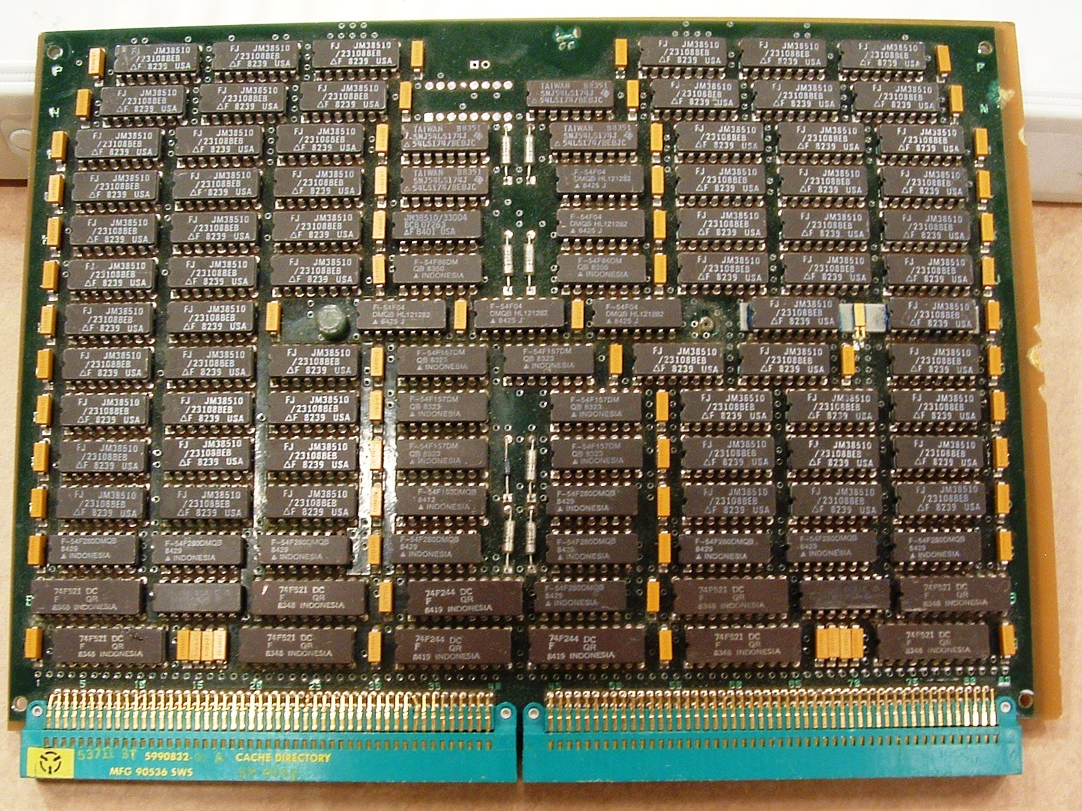 Memory:
The UYK-43 made major advances in storage memory technology through the usage of much faster semiconductor memory technology versus the previous core memories.
This was done for both main memory and cache memory, utilizing the fastest memory technologies available for actual instruction execution.
However, to populate/load that cache, one additional architecture innovation had to be developed and that was to do multiple memory references simultaneously
in anticipation of the processor needing that information. This had never been done before and became an industry standard approach used today.
Memory card shown at the right is in the Lawshe Memorial Museum
artifact collection.
Memory:
The UYK-43 made major advances in storage memory technology through the usage of much faster semiconductor memory technology versus the previous core memories.
This was done for both main memory and cache memory, utilizing the fastest memory technologies available for actual instruction execution.
However, to populate/load that cache, one additional architecture innovation had to be developed and that was to do multiple memory references simultaneously
in anticipation of the processor needing that information. This had never been done before and became an industry standard approach used today.
Memory card shown at the right is in the Lawshe Memorial Museum
artifact collection. - Fault Tolerance and Recovery: Never before, had a computer been architected to be able to diagnose, isolate, and reconfigure itself so it could stay operational, and then inform its human operators of the situation so they could make effective repairs without impacting the overall system operation.
- Input/Output: The UYK-43 was recognized throughout the computer industry as being one of the very best at quickly and efficiently bringing in large amounts of external sensor and other data. Then, after the central processors make the appropriate calculations and determinations, get that information to a human quickly. In situations when an incoming missile or aircraft is threatening a vessel, microseconds become critical. Making timely, accurate, quick decisions saves lives!
- Technology Insertion: From inception, technology insertion was part of the Navy’s plan and supported by Sperry. During its life cycle, multiple technology upgrades were planned and made available. This was made possible by the increased speed, complexity, and capacity of the semiconductor technologies, including larger gate arrays and memory capacity. A few of the upgrades included: higher performance processor and Input/Output Controller (IOC), higher capacity and faster memories, and the optional Tactical Control System (TCS) coprocessor for the submarine community and other users. The support software was also updated to take advantage of the increased capabilities and performance.
- Manufacturing: None of the above could have been accomplished without taking all of the innovative design approaches to “practice” and being able to efficiently and cost-effectively produce computers as required by the Navy. New methods for printed circuit board and cable manufacturing had to be created. LSI fabrication techniques pushed the state-of-the-art of silicon fabrication. New approaches to electronic assembly, integration, and testing were conceived and put into practice daily to produce a reliable product for the Navy. Many of today's accepted Lean Six Sigma methods and practices were started on projects like the UYK-43. [John Westergren]
- Reliability: The UYK-43, because of its cooling system design meeting the Navy’s initial requirements, has been recognized for having very high reliability. According to Sperry/Lockheed Martin Quality personnel, based on Navy data around 2010 the UYK-43 was the most reliable computer in the Navy combat systems.
It remained in use over 30 years (and counting) after its original design, which is unparalleled in commercial computing and processing technology.
Imagine still being able to effectively use a processor that you were using 30, 20, or even 10 years ago.
The innovative architecture that stretched the bounds of memory, large-scale circuit integration, packaging, cooling, and manufacturing technology
came out of close cooperation between the U.S. Navy customer and the Sperry-UNIVAC development team.
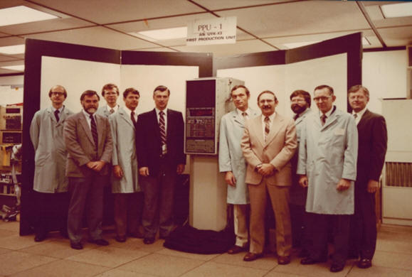 Production unit team leaders are pictured at the right, note the three authors.
- Left Side: Dave Kaminski, Bob Jablonski, John Westergren, Tom Krocheski, Fred Sauer
- Right Side: Gary Hokenson, Jim Bratsch, Doug Wiedenman, Don Fodness, Paul Richardson
- Other Key Engineering Personnel Not Pictured: Jack Metzger, Finley McLeod, Dale Wandersee, Jerry Pertl, Roy Brandenburg, many talented engineering personnel, BJ Bertram, and the Software Group.
3.5.3 Deliveries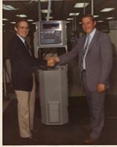
In May 2012 we had posted a synopsis of the AN/UYK-43 Computer written by Unisys/Lockheed Martin engineer David Shelander, https://vipclubmn.org/Articles/AnUyk43Computer.pdf. That paper includes a scanned 1984 letter from J. A. Mallonee, US Navy AN/UYK-43 Project Manager. Mr. Mallonee, left in the picture at the left, shakes Jerry Nickel’s hand, Jerry was on Don Dunn's Sperry UNIVAC program management team.
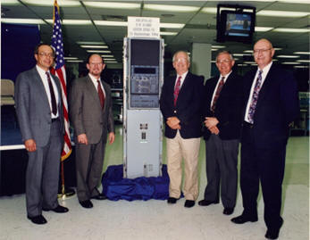 AN/UYK-43 Serial # 1,000 was delivered September 13, 1994 – a decade after the first delivery in 1984.
Left to right were Robert 'Bob' Barushevski
(?sp), Naval Sea Systems
Command (NSSC); Ernie Martaga, Advanced Physics Lab (APL) at Johns Hopkins University; Ken Wander, APL;
Joe Mallonee, NSSC; and Dave Watson, NSCC.
AN/UYK-43 Serial # 1,000 was delivered September 13, 1994 – a decade after the first delivery in 1984.
Left to right were Robert 'Bob' Barushevski
(?sp), Naval Sea Systems
Command (NSSC); Ernie Martaga, Advanced Physics Lab (APL) at Johns Hopkins University; Ken Wander, APL;
Joe Mallonee, NSSC; and Dave Watson, NSCC.
Ship Classes utilizing the AN/UYK-43 were: SSBN Ohio Class Ballistic Missile Submarines; SSN Los Angeles Class Attack Submarines;
DDG Arleigh Burke Class Destroyers; CGN Virginia Class Guided Missile Cruisers.
In addition AN/UYK-43 sales were also made to the Japanese, Australian, Taiwanese, German. and the Norwegian Navy's.
[Doug Wiedenman]
The authors of this cp32bit.html Computers Chapter 55, section 3.5 updated November 2025, are proud to have been part of this Sperry-UNIVAC AN/UYK-43
Excellence in Engineering! Thanks to Bob, Doug, and John for providing this update to our Legacy Anthology,
Thanks to Mary Beth, VIP Club newsletter editor, for sentence and
punctuation error corrections - A variation of this computer chapter
section is the Our Stories for
December 2025.
3.5.4 Enduring Legacy
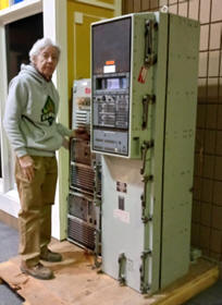 There is an AN/UYK-43 on display at the Lawshe Memorial Museum in S. St. Paul, MN – shown with volunteer Bob Pagac.
The Museum also has a history poster “The Enduring Legacy of the Naval Tactical Data System”,
https://vipclubmn.org/EngDocImg/15.%20Q-70.pdf which includes some AN/UYK-43 summary information.
Part of the text thereon is: “First put to use in 1984 these computers are gradually being replaced by AN/UYQ-70 units,
https://vipclubmn.org/cpothers.html#Q69-70.
However, some UYK-43s will remain in service into the 2020s.”
A bit of irony is that in the late 70s, the UYK-7 enhancement studies
project contracted with two University of Minnesota professors, Dr.
Peter Paton and Dr. Bill Franta, to do cache memory performance studies.
They used Fortran software executing on the CDC 1604 to obtain performance
results for several cache architecture designs. These studies provided
data to help design the AN/UYK-43 system and to solve a subsequent cache
memory 'I/O flushing' problem in the commercial 1110 computer series.
Lowell Benson was the engineering manager responsible for interfacing
with the University. Dave Kaminski was the lead design engineer - he
later was one of the AN/UYK-43 design engineers. [lab]
![]()
4.0 Memory Processor by Dick Erdrich
I should note here that when I did the 'architecture' for the Memory Processor to replace the CP-890 I created a design with 24 bits of addressing. We delivered two processors and a common memory rack containing 8 MB in each of the Trident Memory Processors. Two processors could easily share a common memory due to the presence of extremely large Cache Memories in front of both processors. Commercial processors at the time were only using level 1 caches [level 2 was not here yet] of 256 bytes. Each Memory processor CPU had a 256K byte cache. That was all done in the early 80's. [rae]
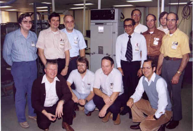
Shown at the right is the engineering development team, photo submitted by Jim Frazier.
- Kneeling in front are Dick Erdrich, Joe Dearing, Neil Macrorie, and Stan Dorr.
- Standing at the left are Bob Litz, John Bergman, and Jim Frazier.
- Standing at the right are Paul Rodriguez, Bill Zekoff, Marv Janisch, Jim Hadine, and Mel Janisch.
Memory Processor: The ‘Memory Processor’ was a 32-bit machine that was used to provide real-time navigation data to the Improved Accuracy Program targeting computer in the Trident II Missile system. I designed the architecture based on the type of data needing manipulation and included some unique capabilities not available elsewhere. It looked a little like a greatly expanded UNIVAC Type 1616 structure with 4 sets of 32 general registers of 32 bits each. The 30 bit CP-890 software could be run by using a cross-compiler written by Sperry Systems Management (SSM). The first demonstration of the Memory Processor was done running the existing the Trident I navigation code. The support software was written by SSM and was based on the Pascal Standard. The eventual High Order Language, when certified, was ADA. When I designed the architecture I took classes in ADA usage and noted that the generated code liked to use pointers to the extent that they would often use nested pointers. To allow this to happen without slowing execution down, I created a pipeline for instruction and operand address generation. We had overlapped executions in many of our earlier machines but this was the first time to my knowledge that a three stage pipeline was used.
Each register set was tied to a context state: Hardware, Executive,
Supervisory, and Task. Context switching took place by instruction or
during an interrupt scan. Being an interrupt driven system, I concentrated
on keeping context switching time to a minimum. The number of registers
was required by the fact that the critical processing was done on complex
floating point values with a pair of registers holding the real component
and another pair holding the imaginary value. This got even trickier
when we went to double length (64-bit) operations. These weren't used
very often but when concluding the final navigation solution all of
those numbers to the right of the decimal point became important. The
instruction set included a full suite of trigonometry functions and
the indexing was optimized for matrix operations. One of our goals was
to complete a 1024 point complex Fast Fourier Transform in under ...
This is just a sample of what that machine had in it. I could go on for hours talking about the huge memory, the huge cache memory, the first implementation of Mil-Std-1553 serial on a non-airborne platform, the fully programmable I/O configuration capability, etc. But that’s probably for another day.
Cheers, Dick.
![]()
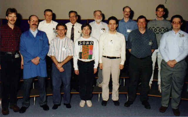
Shown at the left is the checkout and test crew. Helping Lowell [lab] with the face identifications were Dan Reiman [dbr], Dick Lundgren [rfl], Paul Mahowald [pm], and Larry Bolton [lb] - Thanks guys
From left to right they are:
Brent Anderson dbr, Paul Mahowald rfl, Paul Dietzler lab, Brian Newman lb, Paul Rodriguez lab, Greg Berger dbr, Jim Frazier lab, Dan Reiman lab, John Justin dbr, John Bergman dbr [Cecil Metz's brother-in-law lab], Dan Gilbertson dbr, and Dave Smith pm.5. Repertoire Cards
Many people gave repertoire cards to the Legacy Committee. Keith Myhre scanned the cards before they were donated to the Charles Babbage Institute. The 32-bit cards are linked hereunder. There are copies of many of these cards at the Lawshe Memorial Museum.
- NAVSEA 0967-LP-024-5800 AN/UYK-7(V) Technical Summary Handbook
- AN/UYK-7 Computer Repertoire of Instructions, ten pages
- AN/UYK-7 Repertoire of Instructions, 4 page
- AN/UYK-7 Repertoire of Instructions, 6 page - May 1971
- AN/UYK-7 Repertoire of Instructions, 6 page
- AN/UYK-7 Repertoire of Instructions
- AN/UYK-7(V) Diagnostic Supplementary Tests & Operating Instructions
- S-3A Sperry Univac 1832 Technical Summary (UDS77648)
- UNIVAC 1832
Repertoire of Instructions
6. Technical Manuals
The bit-savers web site (http://bitsavers.informatik.uni-stuttgart.de/) has over 32,000 documents. We've copied the 32-bit ISA documents and linked them hereunder for technology researchers ease of access.
- CMS-2Y Programmers Reference Manual for the AN/UYK-7 and AN/UYK-43 Computers
- M100091-C Compiler Monitor System-2 (CMS-2) for use with AN/UYK-7 Computer
- PX5652E AN UYK-7 Technical Description
- UX5073 AN UYK-7(V) Brochure - The Next Generation
In this Chapter
- Introduction [left]
- Computer Family
- 32 bit descriptions [below]
- Memory Processor
- Repertoire Cards
- Technical Manuals
Chapter 55 edited
1/5/2026.
![]() |
Home, Pg 1 |
Our Legacy, Ch 1 |
People |
Locations |
Engineered |
Computers |
Systems |
Contacts and Links |
Site Map, Pg 0 |
|
Home, Pg 1 |
Our Legacy, Ch 1 |
People |
Locations |
Engineered |
Computers |
Systems |
Contacts and Links |
Site Map, Pg 0 |
Copyright ©2025, LABenson for the VIP Club. All Rights Reserved; Hosted on www.webhostinghub.com since 2011.